 | –≠–ª–µ–∫—Ç—Ä–æ–Ω–Ω—ã–π –∫–æ–º–ø–æ–Ω–µ–Ω—Ç: AN7560 | –°–∫–∞—á–∞—Ç—å:  PDF PDF  ZIP ZIP |
ICs for Audio Common Use
1
AN7560Z
BTL output power IC for car audio
s
Overview
The AN7560Z is an audio power IC developed as the
sound output of car audio (35 W by 4-ch.). A capacitor
and resisitor to stop oscillation are built in between the
output pin and GND so that a space saving of set is pos-
sible. Also, it incorporates a perfect muting circuit with-
out shock noise so that a shock noise design under the set
transient condition can be made easily when used together
with its standby function. In addition, it incorporates var-
ious protection circuits to protect the IC from destruc-
tion by GND-open-shortcircuit to ground and power sup-
ply surge which are the important subject of power IC
protection. This IC will largely contribute to a high reli-
ability design of the equipment.
s
Features
∑
A pattern layout in which input and output pattern do
not intersect each other on single-sided printed circuit
board is possible.
∑
Incorporating various protection circuits (temperature,
shortcircuit to V
CC
, V
CC
-open short circuit to V
CC
,
shortcircuit to GND, GND-open short circuit to GND,
overvoltage, power supply surge, and ASO, etc.)
∑
Built-in standby function (shock noise-free when STB-
on/off)
∑
Built-in muting function (shock noise-free when Mute-
on/off)
∑
External components reduction
∑
Provided with beep sound input pin
∑
Equipped with auxiliary sound input pin
s
Applcations
∑
Car stereo, miniature audio component, karaoke and
other audio equipment.
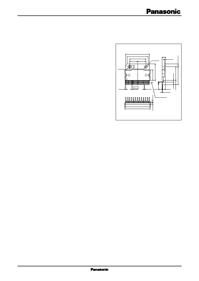
Unit: mm
HZIP025-P-0980
(10.50)
(10.50)
21.0±0.1
1.5±0.1
27.0±0.3
4.5±0.2
31.0±0.3
3.6±0.1
14.5±0.3
(1.95)
(2.15)
15.5±0.3
(3.30)
2.4±0.5
(5.70)
18.75±0.30
(24.45)
3.75±0.10
(1.26)
0.40
+0.2
≠0.1
+0.15
≠0.05
Seating plane
3.6±0.1
R1.8±0.1
0.6
(5.08)
(4.29)
1.27
1
25
33.0±0.3
33.36±0.30
2
AN7560Z
ICs for Audio Common Use
Pin No.
Description
1
ch.4 Output (
+
)
2
GND (Output ch.4)
3
ch.4 Output (
-
)
4
V
CC
5
ch.3 Output (
+
)
6
GND(Output ch.3)
7
ch.3 Output (
-
)
8
GND (Output ch.2)
9
ch.2 Output (
+
)
10
Auxiliary sound input
11
ch.2 Output (
-
)
12
V
CC
13
ch.1 Output (
+
)
s
Absolute Maximum Ratings
Parameter
Symbol
Rating
Unit
Supply voltage
*2
V
CC
25
V
Peak supply voltage
*3
V
surge
65
V
Supply current
I
CC
12
A
Power dissipation
*4
P
D
59
W
Operating ambient temperature
*1
T
opr
-
30 to
+
85
∞
C
Storage temperature
*1
T
stg
-
55 to
+
150
∞
C
Note) *1 : All items are at T
a
=
25
∞
C, except for the operating ambient temperature and storage temperature.
*2 : Without signal
*3 : Time
=
0.2 s.
*4 : Power dissipation at T
a
=
85
∞
C.
Pin No.
Description
14
GND(Output ch.1)
15
ch.1 Output (
-
)
16
Standby
17
ch.1 Input
18
Beep Sound Input
19
ch.2 Input
20
GND (Input)
21
ch.4 Input
22
GND (Sub)
23
ch.3 Input
24
Muting
25
Ripple Filter
s
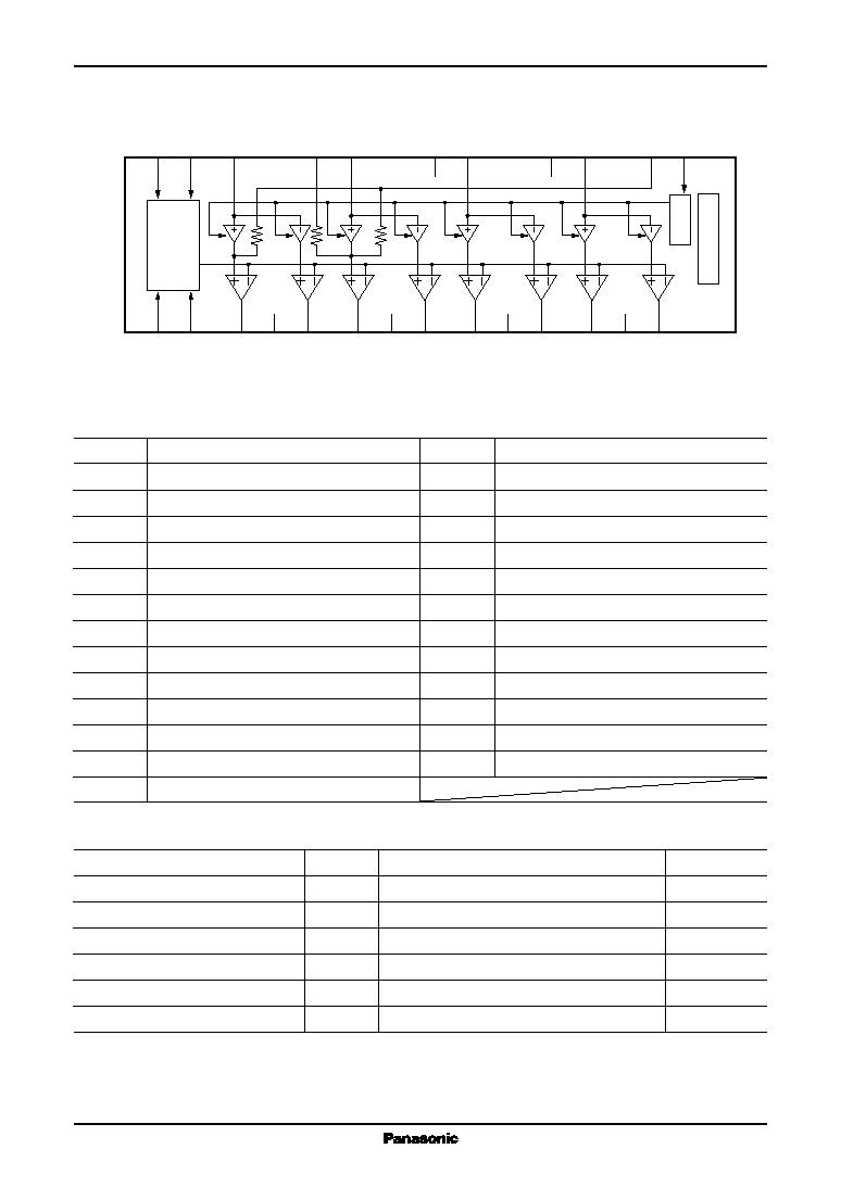
Pin Descriptions
s
Block Diagram
14
15
9
8
11
4
12
16
25
10
19
17
18
24
13
6
7
1
2
3
5
Ripple Filter
ch.1 Input
Aux Input
ch.2 Input
GND
GND
GND
GND
GND
GND
ch.3 Input
ch.4 Input
Beep Input
Muting
Standby
Ripple
Filter
ch.4 Output
ch.4 Output
ch.3 Output
ch.3 Output
ch.2 Output
ch.2 Output
ch.1 Output
ch.1 Output
V
CC
V
CC
22
21
20
23
Att. Con
Protection Cct.
3
ICs for Audio Common Use
AN7560Z
Parameter
Symbol
Conditions
Min
Typ
Max
Unit
Quiescent current
I
CQ
R
g
=
10 k
,
R
L
=
4
300
450
mA
Standby current
I
STB
R
g
=
10 k
,
R
L
=
4
1
10
µ
Output noise voltage
*1
V
NO
R
g
=
10 k
,
R
L
=
4
0.15
0.5
mV[rms]
Voltage gain
G
V
V
IN
=
40 mV[rms],
R
L
=
4
32
34
36
dB
Total harmonic distortion 1
THD1
V
IN
=
40 mV[rms],
R
L
=
4
0.05
0.2
%
Maximum output power 1
P
O1
THD
=
10%,
R
L
=
4
16
19.5
W
Ripple rejection
*1
RR
R
g
=
10 k
,
R
L
=
4
60
68
dB
V
R
=
1 V[rms], f
R
=
1 kHz
Channel balance
CB
V
IN
=
40 mV[rms],
R
L
=
4
0
1
dB
Cross-talk
CT
R
g
=
10 k
,
R
L
=
4
60
70
dB
V
IN
=
40 mV[rms]
Output offset voltage
V
OFF
R
g
=
10 k
,
R
L
=
4
-250
0
250
mV
Muting effect
*1
MT
V
IN
=
40 mV[rms],
R
L
=
4
70
86
dB
Input impedance
Z
I
V
IN
= ±
0.3 V
DC
24
30
36
k
Shock noise
*2
V
S
R
g
=
10 k
,
R
L
=
4
, V
MUTE
=
5 V
-100
0
100
mV[0-P]
V
STB
=
on/off, 50 Hz HPF
Total harmonic distortion 2
THD2
V
IN
=
20 mV[rms], f
IN
=
20 kHz
0.1
0.5
%
R
g
=
10 k
, R
L
=
Mute On threshold voltage
MT
ON
V
IN
=
40 mV[rms],
R
L
=
4
4
V
Mute Off threshold voltage
MT
OFF
V
IN
=
40 mV[rms],
R
L
=
4
0.8
V
Maximum output power 2
P
O2
V
IN
=
1 V[rms],
R
L
=
4
28
W
Maximum output power 3
P
O3
V
CC
=
14.4 V, THD
=
10%,
R
L
=
4
21
W
Maximum output power 4
P
O4
V
CC
=
14.4 V, V
IN
=
1 V[rms],
34
W
R
L
=
4
s
Electrical Characteristics at V
CC
=
13.2 V, f
=
1 kHz, T
a
=
25
∞
C
s
Recommended Operating Range
Parameter
Symbol
Range
Unit
Supply voltage
V
CC
8.0 to 18.0
V
Note) *1 : Measurement using a bandwidth 15 Hz to 30 kHz (12 dB/OCT) filter.
*2 : Change over the standby terminal at the time shown in the right.
5 V
0 V
500 ms
500 ms
4
AN7560Z
ICs for Audio Common Use
Ambient temperature T
a
(∞
C)
Po
wer dissipation P
D
(W)
100
113.6
120
0
25
150
50
75
100
125
80
60
59.5
40
40.3
20
4.02
20.5
0
Without heat sink
5
∞
C/W heat sink
2
∞
C/W heat sink
1
∞
C/W heat sink
Infinite heat sink
Independent IC
without heat sink
R
thj-c
=
1.1
∞
C/W
R
thj-a
= 3
1.1
∞
C/W
s
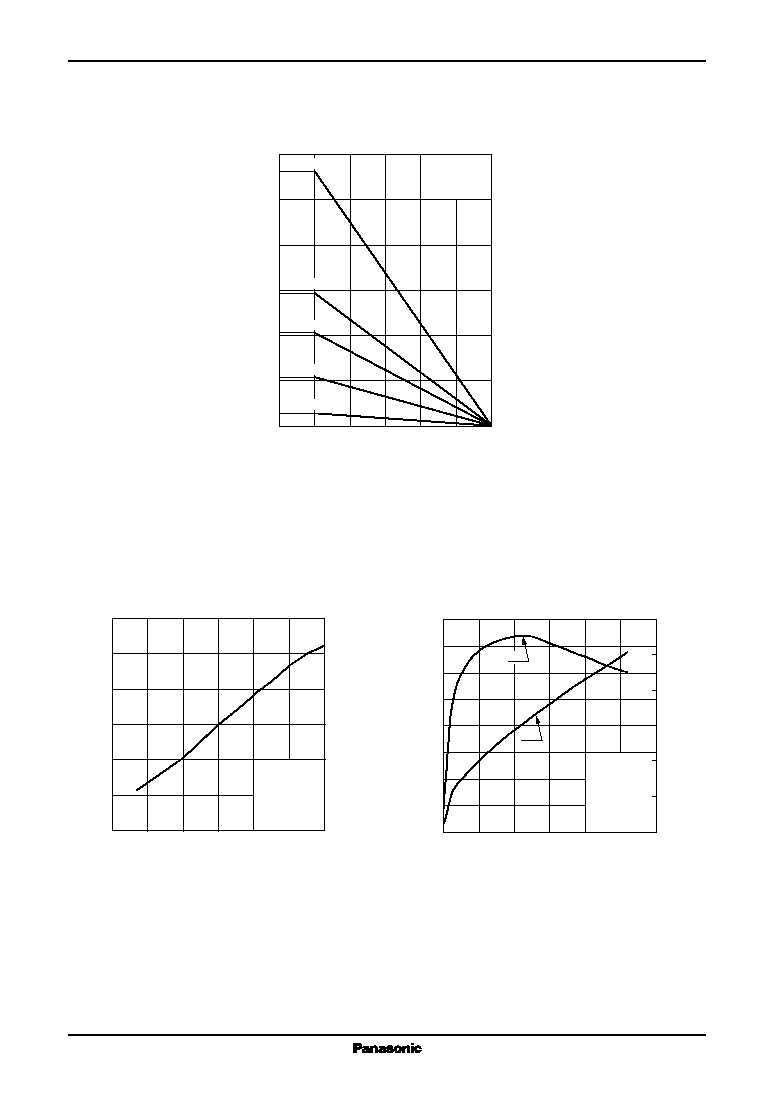
Technical Information
1. P
D
T
a
curves of HZIP025-P-0980
P
D
T
a
6
8
10
12
14
16
18
0
5
10
15
20
25
30
Supply voltage V
CC
(V)
freq
=
1 kHz
THD
=
10
%
R
L
=
4
400 Hz HPF
30 kHz LPF
4-ch. input
R
g
=
10 k
Output power
P
O
(W)
0
5
10
15
20
25
30
0
2
4
6
8
10
12
0
5
10
15
20
25
30
35
40
Power consumption P
C
(W)
P
C
I
CC
Output power (1-ch.) P
O
(W)
Supply current I
CC
(A)
V
CC
=
13.2 V
freq
=
1 kHz
R
L
=
4
400 Hz HPF
30 kHz LPF
4-ch. input
R
g
=
10 k
2. Main characteristics
P
O
V
CC
P
C
, I
CC
P
O
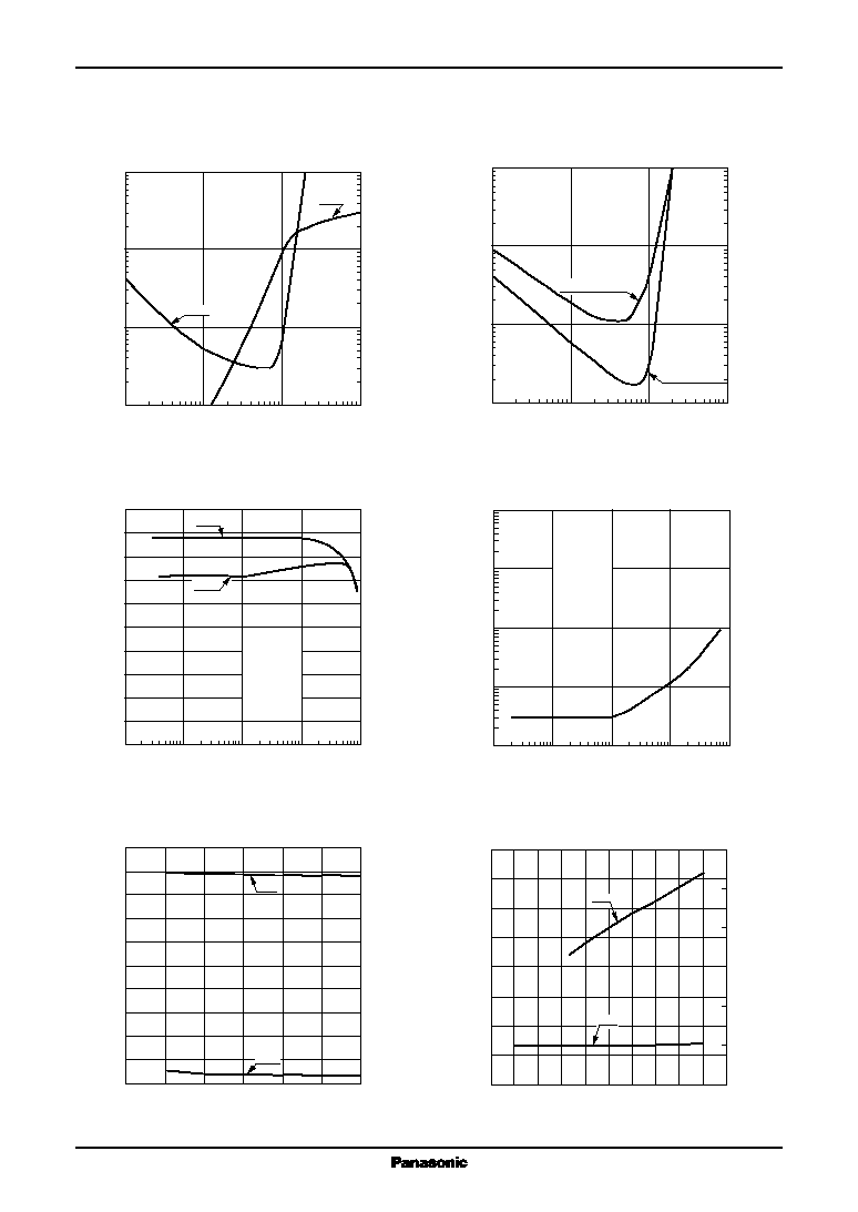
5
ICs for Audio Common Use
AN7560Z
0
2
4
6
8
10
12
20
14
16
18
Supply voltage V
CC
(V)
Standby current I
STB
(
µ
A)
Quiescent circuit current
I
CQ
(A)
0
50
100
150
200
250
300
350
400
-
2
0
2
4
6
8
10
I
STB
I
CQ
6
8
10
12
14
16
18
25
26
27
28
29
30
31
32
33
34
35
0.0
0.1
0.2
0.3
0.4
0.5
0.6
0.7
0.8
0.9
1.0
G
V
THD
Supply voltage V
CC
(V)
Voltage gain
G
V
(dB)
Total harmonic distortion
THD
(
%
)
P
O
=
1 W
1
10
100
1 000
Input voltage V
IN
(mV[rms])
Output power P
O
(W)
0.01
0.1
1
10
Total harmonic distortion THD (
%
)
P
O
V
CC
=
13.2 V
freq
=
1 kHz
R
L
=
4
400 Hz HPF
30 kHz LPF
4-ch. input
R
g
=
10 k
THD
0.1
1
10
100
1
10
100
1 000
Input voltage V
IN
(mV[rms])
Total harmonic distortion
THD (
%
)
0.01
0.1
1
10
THD f
IN
=
100 Hz
THD f
IN
=
10 kHz
V
CC
=
13.2 V
freq
=
100 Hz,10 kHz
R
L
=
4
400 Hz HPF
30 kHz LPF
4-ch. input
R
g
=
10 k
s
Technical Information (continued)
2. Main characteristics (continued)
P
O
, THD
V
IN
THD
V
IN
G
V
, P
O
freq
THD
freq
25
26
27
28
29
30
31
32
33
34
35
10
100
1 000
10 000
100 000
0
5
10
15
20
25
Frequency freq (Hz)
Voltage gain
G
V
(dB)
Output power
P
O
(W)
V
CC
=
13.2 V
P
O
=
1 W
THD
=
10%
R
L
=
4
400 Hz HPF
30 kHz LPF
4-ch. input
R
g
=
10 k
P
O
G
V
0.01
0.1
1
10
100
10
100
1 000
10 000
100 000
Frequency freq (Hz)
Total harmonic distortion THD
(
%
)
V
CC
=
13.2 V
P
O
=
1 W
R
L
=
4
400 Hz HPF
30 kHz LPF
4-ch. input
R
g
=
10 k
G
V
, THD
V
CC
I
CQ
, I
STB
V
CC